Lynford Goddard
 Multi-depth Atomic Layer Etching of Silicon using Photo-Electro-Thermo-Chemistry
The amazing communications, computing, and information gathering capabilities of your smart phone are made possible by the continual exponential increase in the number of transistors in the microprocessor that was fabricated on a silicon wafer. Currently, these transistors are each roughly only 20 atoms wide by 100 atoms long by 20 atoms tall in size. If the manufacturing process (silicon etching) produces transistors that are just a single atomic layer too thin or too thick, the error in device dimension would be 5%. This is a huge error and enough to noticeably deteriorate the overall performance of the entire microprocessor. Therefore, controlling the etch depths in the silicon wafer with an accuracy of a single atomic layer is critical.
Currently, the semiconductor manufacturing industry relies on a binary process for etching. Some wafer regions are exposed to a chemical or physical reaction and thereby etched to a specific depth while other regions are covered and not etched at all. It is not possible to etch to a depth in between these two values in a single step. This stifles the creativity of modern engineers because they are limited to using architectures that are 2D or quasi-3D. They do not have continuously varying height structures in their device design palette.
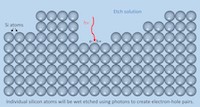
This project explores using high speed optical, electrical, and thermal effects to realize a new approach for atomic layer etching. It seeks not only to address the grand challenge of controlling the etch depth with atomic layer accuracy but also to enable this depth to be varied across the wafer surface. Professor Goddard will use his CAS appointment to work in the lab with his graduate and undergraduate research students to design, build, and characterize a prototype system.
