Jean-Pierre Leburton
 Genomics with Semiconductor Nanotechnology
Over the past few years the need has grown for low-cost, high speed, and accurate biomolecule sensing, propelling the so-called third generation of genome sequencing devices. Many associated technologies have been developed, but recent advances in semiconductor nanotechnology have opened new avenues in the field. While it is possible to fabricate solid-state structures with dimensions comparable to the separation between atoms in bio-molecular systems, progress in mesoscopic physics has demonstrated sensing capabilities of nanoscale capacitors corresponding to a fraction of the electron charge. This in principle enables probing single biomolecules electrically.
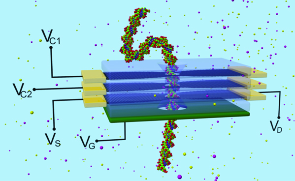
In this context, the idea of engineering nanopores (i.e., small aperture of nanometer feature sizes in ultra-thin solid-state membranes to mimic the operation of biological ion channels in living cells) has emerged to investigate biological processes with semiconductor nanotechnology. Indeed, the versatility of semiconductor materials in terms of conduction polarity by selective n-or p-doping, as well as their ability to tailor space charge at the surface provide electrical detection sensitivity for biological objects with new means to shape the electrostatic landscape close to the membrane. During his Center appointment, Professor Leburton will explore the use of multi-layer semiconducting graphene membranes as bio-nanoelectronic devices with enhanced performances and functionality for sensing and manipulation of biological information. Stacking nanoscale layers with different doping, different dielectric properties or individual electrical tunability results in additional degree of freedom for the control, manipulation and detection of bio-molecules along the artificial ion channels. In this scenario, graphene layers manipulate the molecule, while others can locally sense its chemical structure through the charge of its constituents, thereby integrating different functions in a single membrane.
This explorative research will be theoretical in nature by using computational tools that integrate electronic device with atomistic and molecular biophysics simulation into a multi-scale self-consistent scheme.
Schematic diagram of a four-layer device containing two grapheme layers (dark) biased at VC1 and VC2 to control the translational motion of DNA through the nanopore. A third grapheme layer (VDS) measures the sheet current. Finally, a heavily doped back gate (green) lies underneath the sheet current layer to control its conductivity. Oxide barriers (transparent) between different grapheme layers provide electrical isolation.
